Printed circuit boards underpin modern electronics. They connect components in devices from smartphones to industrial machines. Manufacturers follow a series of steps to produce these boards. Each phase requires care to meet quality standards. This post explores the process, highlighting key techniques. Readers in engineering or production will find practical insights. We’ll cover materials, fabrication methods, and quality checks. Understanding these elements helps in selecting suppliers and improving workflows.
Starting with Materials and Design
The process kicks off with design. Engineers use software to layout circuits. They place traces, vias, and pads. Designs account for signal integrity and thermal management. Once finalized, the layout transfers to manufacturing files.
Base materials come next. Fiberglass-reinforced epoxy forms the substrate. Copper foil clings to one or both sides. For multilayer boards, multiple cores stack with prepreg layers. Prepreg is resin-soaked fabric that bonds under heat.
Copper thickness varies. Standard is 1 ounce per square foot, about 35 microns. Thicker copper suits high-current applications. Panels cut to size, often 18 by 24 inches. Cleanliness matters here. Dust or oils can cause defects later.
Preparing the Substrate
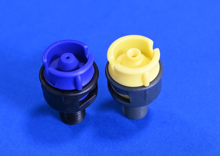
Substrate prep involves cleaning. Brushes scrub off oxides and debris. Nylon filaments work well, flexible yet tough. They remove contaminants without scratching. This step sets up for imaging. Clean boards ensure resist adheres properly.
Drilling registration holes follows. These align layers during stacking. Accuracy is key. Misalignment leads to faulty connections.
Imaging and Pattern Transfer
Imaging defines the circuit. Photoresist coats the copper. It’s light-sensitive. A film negative or laser plots the pattern. UV light exposes the resist. Exposed areas harden.
Development washes away unexposed resist. Alkaline solutions do this in wet lines. Horizontal conveyors move boards through tanks. Spray nozzles apply developer evenly. Rinsing removes residues.
For inner layers, this happens before lamination. Outer layers follow after plating. Precision in imaging allows fine lines, down to 50 microns.
Etching to Form Circuits
Etching strips unwanted copper. Chemical baths dissolve it. Cupric chloride is common, regenerative. Acidic etchants suit some lines.
In horizontal setups, boards pass through etchant sprays. Uniform flow prevents undercuts. Etch factor measures sidewall straightness. High factors mean sharp traces.
Seal strips contain solutions in tanks. They reduce leaks and noise. Post-etch, stripping removes remaining resist. Alkaline baths handle this, followed by rinses.
Drilling and Hole Wall Preparation
Drilling creates holes for vias and components. Mechanical drills use carbide bits. Lasers handle microvias, precise to 0.1 mm.
Deburring smooths burrs. Brushes or high-pressure water jets do this. Smear from drilling resin needs removal. Plasma or chemical desmear cleans hole walls.
Plating for Connectivity
Plating adds copper to holes. Electroless plating starts with a thin layer. It makes walls conductive. Electroplating builds thickness, usually 25 microns.
Additives in the bath control growth. Brighteners and levelers ensure even deposit. Panels agitate for uniformity. Rinsing prevents drag-out contamination.
Applying Solder Mask and Silkscreen
Solder mask protects traces. It’s a polymer coating. Liquid photoimageable types apply by curtain or spray. UV cures the pattern. Openings expose pads for soldering.
Curing bakes the mask. It hardens fully. Colors like green are standard, but options exist.
Silkscreen adds text and symbols. Ink prints via screens. UV or heat cures it. This aids assembly, marking part locations.
Surface Finishes for Protection
Finishes guard against oxidation. Hot air leveling coats with solder. It levels pads. Immersion tin or silver offers alternatives.
Gold over nickel suits fine pitches. Organic preservatives are thin, eco-friendly. Choice depends on shelf life and soldering needs.
Electrical Testing and Routing
Testing checks for defects. Probes verify opens and shorts. Flying probes are flexible for prototypes. Fixtures suit volume production.
Optical inspection scans surfaces. It spots missing features or bridges. X-ray views internal layers.
Routing cuts boards from panels. CNC mills shape edges. V-scoring allows breaking apart. Final checks confirm dimensions.
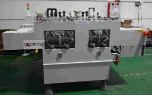
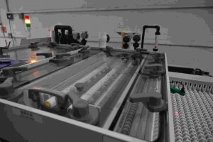
Wet Processing in Horizontal Lines
Wet lines handle many steps. They process boards flat on conveyors. This suits volume runs.
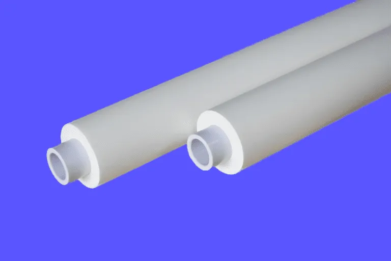
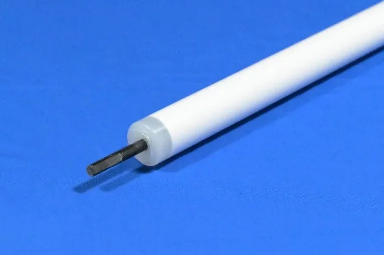
Pre-treatment cleans with brushes. Nylon types remove oxides gently. Sponge rollers absorb water after rinses. They prevent spots.
Developing uses alkaline sprays. Etching follows in sealed tanks. Air knives dry boards post-rinse. High-speed air strips moisture.
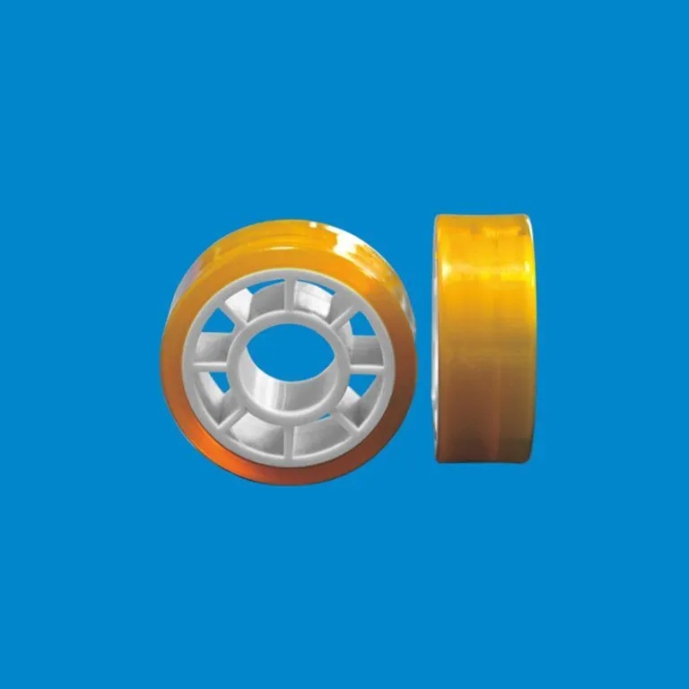
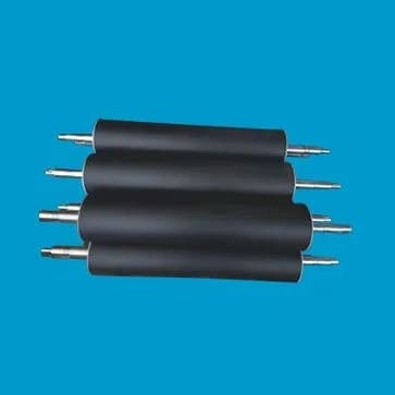
Transmission parts guide boards. U-blocks position accurately. Gears drive smoothly. These components endure chemicals.
Horizontal lines boost throughput. They cut handling, reducing breaks. Modular setups adapt to board sizes.
- Cleaning: Brushes scrub, sponges dry.
- Developing: Solutions dissolve resist.
- Etching: Chemicals pattern copper.
- Rinsing: Water neutralizes.
- Drying: Air knives evaporate water.
Such systems lower costs. They conserve water via cascades. Quality rises with consistent flow.
| Stage | Purpose | Key Equipment |
| Cleaning | Remove contaminants | Brush rollers |
| Developing | Pattern resist | Spray manifolds |
| Etching | Define traces | Etchant tanks |
| Rinsing | Clean residues | Overflow systems |
| Drying | Eliminate moisture | Air knives |
This table shows wet line flow. Each part contributes to board reliability.
Quality Assurance Throughout
Standards guide production. IPC specs set tolerances. Trace widths hold tight. Hole placement aligns precisely.
Bath analysis monitors chemistry. pH and density checks keep solutions effective. Waste treatment handles spent chemicals.
Traceability tracks lots. From raw materials to finished boards. This aids recalls if needed.
Training staff maintains consistency. Audits verify processes. Continuous improvement refines methods.
Shenzhen Qixingyuan Machinery Equipment Co., Ltd.: Supplier of PCB Horizontal Line Wet Processing Spares
Shenzhen Qixingyuan Machinery Equipment Co., Ltd. serves as a key supplier for PCB horizontal line wet processing equipment spares and parts. Founded in 2008, the company combines design, production, and sales. It holds several national patents, focusing on components that enhance wet segment efficiency.
Their range includes air knives for drying, brush and sponge rollers for cleaning, seal strips for etching tanks, and transmission items like U-blocks and gears. Materials resist corrosion, suiting acidic or alkaline conditions. Customization fits line speeds and board dimensions.
With a 50,000 square meter facility and over 300 employees, they produce millions of units yearly. Exports reach Europe, Asia, and the Americas. One-stop services cover design to installation. Flexible order quantities and quick delivery—often within seven days—support small and large buyers. Agents highlight marketing aid and competitive pricing. This positions the firm as a dependable source, helping manufacturers maintain uptime and precision in PCB production. Their focus on innovation and quality builds long-term partnerships.
Conclusion
PCB manufacturing blends materials science with precise engineering. Wet processing stands central, shaping circuits reliably. Grasping these steps aids in better production choices. Suppliers play a vital role, providing parts that sustain quality.